
Weijin Research/Envision Energy/Yicai
Shanghai
Joined March 2016
- Tweets 5,317
- Following 1,672
- Followers 205
- Likes 116
scott retweeted

Designing an inference chip for robots is actually very difficult.
In data centers each chip is bathed in jacuzzi and babysat by nannies. If they died it would be hot swapped by one of their clones.
The fault rate of GPUs in datacenter is actually quite high. Industrial average annual fault rate of H100 is 9%. Ideal conditions could reduce it down to 2% but never below a single digit.
The fault recovery of GPU nodes actually could take a while, from minutes to hours. It is not instantaneous.
In robots, the chips are out in the cold and they need rapid self recovery. The fault tolerance is in a different league. It is not uncommon many robotic companies struggle to get the chip running more than a few hours without rebooting.
For chip companies, this is great since they would tell robotic companies to buy more chips for hot swapping.
For robotic companies, this is bad since it is obviously not a scaleable solution but they are stuck with endless back-and-forth JIRA tickets with vendors.
scott retweeted

Energy, Entropy and Exergy
Everyone knows what energy is, about 1 in 200 people know what entropy is, and about 1 in 500 people know what exergy is.
Learning these terms makes it far easier to understand and compare various energy technologies and energy sources, because a lot of the lexicon used in public / media is terrible, clumsy and just wrong. This leads to a lot of people advocating bad ideas.
First of all Exergy
Exergy is just the useful work that you can get out of a system. Think of it as the fraction of the energy that you can actually monetise.
Different primary energy sources and heat engines all have different exergy mechanics.
A 50MW solar farm and a 50MW gas turbine have very different exergy outputs and it’s the exergy that is the useful work that we can monetise. Capacity is kinda a meaningless dumb point of comparison when neither operates at capacity.
So for a barrel of oil, the exergy is the work done to push your car forward after the oil is refined into gasoline and burnt in the engine. This is a much smaller number than the energy content of the barrel. Same applies to a wind turbine.
Exergy is the thermodynamic term that a finance team should care about. Learn it.
Exergy weighted comparisons should drive capital allocation decisions.
Next is entropy
You will see a lot of people try and describe this as “disorder” or “irreversibility” or other confusing ways to communicate entropy.
Let me keep it simple, entropy is the fraction of energy that is not exergy. Entropy is the part of the energy that you cannot use, it produces no useful work, you cannot monetise it.
Entropy is basically the energy that your system consumes internally to drive itself through a continuous process (technically inaccurate ELI5 version).
Entropy manifests as a cloud of steam floating out of a cooling tower, you cannot reverse it, you can’t unmake your omelette.
Entropy is all the pipes in your power plant getting hot and wasting heat, it’s the noise of your pumps, etc.
For some reasons physics demands every energy conversion process must waste some energy, sometimes it’s not much, sometimes it’s a lot.
Another way to think of entropy is as an impact on the environment, because it’s a change you are putting into the environment not because you want to, but as a byproduct of monetising your exergy.
Really we want high exergy low entropy technologies and we want a lot of them.
So I like (exergy^2 / entropy) as a comparison metric of a system that captures both its quality and its scale.
See the diagram below, don’t over complicate things if you don’t need to. Unless your job is to design turbine blades this energy, exergy, entropy framework is fine and very useful.

scott retweeted

🔵Tokyo Electron : The future of AI hardware will be defined by the convergence of physical scaling and heterogeneous integration. Transistor innovation alone is no longer enough. System performance now comes from co-optimizing logic, memory, interconnect, and advanced packaging as a unified architecture.
GAA and CFET push logic scaling forward. Backside PDN improves power delivery. 4F² VCT and 3D DRAM continue density scaling. Yet the real breakthrough comes when everything is integrated: GPU/CPU cores surrounded by HBM, connected through 3DIC structures, and supported by ultra-flat wafers, known-good dies, and high-efficiency heat spreaders.
This is the new era of AI semiconductors.
The bottleneck has shifted from transistor count to how fast we can move data, stack memory, reduce thermal resistance, and pack heterogeneous functions into one compute engine.
The next performance leaps won’t come from one domain. They will come from cross-domain integration.
SemiVision

scott retweeted

Exciting big Kimi K2 Thinking release!
More experts, fewer heads, and even more thinking!


🚀 Hello, Kimi K2 Thinking!
The Open-Source Thinking Agent Model is here.
🔹 SOTA on HLE (44.9%) and BrowseComp (60.2%)
🔹 Executes up to 200 – 300 sequential tool calls without human interference
🔹 Excels in reasoning, agentic search, and coding
🔹 256K context window
Built as a thinking agent, K2 Thinking marks our latest efforts in test-time scaling — scaling both thinking tokens and tool-calling turns.
K2 Thinking is now live on kimi.com in chat mode, with full agentic mode coming soon. It is also accessible via API.
🔌 API is live: platform.moonshot.ai
🔗 Tech blog: moonshotai.github.io/Kimi-K2…
🔗 Weights & code: huggingface.co/moonshotai

scott retweeted

BREAKING: Leaked October 27 letter from OpenAI to White House shows that
• OpenAI had begun asking for Federal guarantees over a week ago.
• Sam’s long attempted walkback yesterday on X after the huge backlash was a total lie.
You cannot trust this man, ever.
That’s what Ilya saw.


scott retweeted

The claim that China will account for 45 percent of global manufacturing in 2030 has gained surprising traction, despite the fact that it is completely implausible.
The statistic comes from a 2024 UN Industrial Development Organization (UNIDO) report on the future of industrialization. Inexplicably the authors chose to extrapolate a linear trend from 2024 to 2030 … based on average growth rates from 2010 to 2019.
When using more reasonable assumptions, it quickly becomes clear just how far-fetched the idea of China reaching a 45% share of global manufacturing truly is—especially given how sharply it diverges from the current best-fit trajectory.
Below are three scenarios: the UN’s projection (which requires a 1.2 percentage point annual increase), a best-fit extrapolation, and a bear case that assumes a 0.6 percentage point decline per year.


scott retweeted

Quantinuum unveiled Helios, a trapped-ion system delivering 48 logical error-corrected qubits from 98 physical—a striking 2:1 ratio that boosts reliability and puts real commercial use cases within reach.
The launch pairs with Guppy, a new language so algorithms built today can scale to future machines, and early users like JPMorgan Chase are already running more complex workloads.


Solid State Battery is going to come from consumer products b4 EVs. XPeng robot will be among many products that get SSB next yr.
Look at BYD battery page, it shows solid state electrolyte as one of the advanced techs in its product line. It will have SSB for consumer products in 2026.
Among others, it also has ultra-thin high-viscosity separator & HV LiCobalt, High-ED ternary, LMFP, SIB cathode & Fast-Charging stearate, High-ED Si Anode.

scott retweeted

🔥 GPT-6 may not just be smarter.
It literally might be alive (in the computational sense).
A new research paper, SEAL: Self-Adapting Language Models (arXiv:2506.10943), describes how an AI can continuously learn after deployment, evolving its own internal representations without retraining.
Here are the details: 🧵

scott retweeted

“Hybrid bonding expected to be introduced after HBM4E… needs to happen faster”
There is a view that hybrid bonding technology, known as a next-generation packaging technology for high-bandwidth memory (HBM), will be introduced after the 7th-generation HBM4E. The basis is that hybrid bonding equipment is costly and difficult to localize domestically, and that the existing thermo-compression (TC) bonding technology can still cope for now.
On the 7th, Joo Seung-hwan, a professor at Inha University’s Graduate School of Manufacturing Innovation, said, “The introduction and application of hybrid bonding equipment will take place around HBM4E or HBM5,” adding, “Equipment makers are making similar predictions.”
Professor Joo said, “The biggest reason hybrid bonding is not applied now is cost,” adding, “Besi, the leader in the bonding equipment industry, has developed hybrid bonding equipment with Applied Materials and is supplying it to TSMC, but the equipment price is quite expensive.” He added, “Domestic equipment companies are trying to localize at a relatively lower price range, but the technology is not yet ready.” In October, Besi and Applied Materials completed development of the die-to-wafer hybrid bonding equipment “KineX Bonding System.” The price of this equipment is said to be in the range of KRW 15–20 billion.
Professor Joo said, “Moreover, the industry believes that even with TC bonding alone, HBM can be stacked up to 33 layers,” adding, “Since HBM4/4E as well as the 8th-generation HBM5 are at the 20–24-high level, there is no compelling reason to use hybrid bonding.” According to data from market research firm Yole Group, HBM manufacturing is expected to move from the currently used TC bonding to fluxless TC bonding that uses no chemicals/adhesives (flux). It will then go through a Cu-Cu direct approach that connects copper to copper and move into hybrid bonding.
Professor Joo said, “The main reason for adopting hybrid bonding for HBM is heat,” noting, “If you manufacture HBM with hybrid bonding, thermal efficiency improves by about 100 times.” He continued, “Because HBM stacks multiple memory chips vertically, the more chips there are, the greater the heat problem,” and emphasized, “As the HBM stack height increases and the number of through-silicon vias (TSVs) rises, the likelihood of applying hybrid bonding grows.”
TSVs are the channels that vertically connect DRAM. An increase in the number of TSVs means these interconnect channels become denser. In the TC bonding method, these channels are connected with tiny metal spheres (micro-bumps). Hybrid bonding directly connects the copper wiring and dielectrics of the chips without micro-bumps, allowing the TSV pitch to be reduced to below a few micrometers (μm).
Professor Joo said, “Up to 16-high HBM, I believe heat can be managed even with TC bonding,” while adding, “When HBM goes from 20–24-high to 24–28-high and the number of TSVs doubles, hybrid bonding will be unavoidable.” He further noted, “According to Besi’s materials, hybrid bonding can improve HBM speed by 11.9 times and connection density by 15 times compared to conventional TC bonding.”
SK hynix Executive Vice President Kang-wook Lee also stated at an academic event hosted by the Korean Institute of Electronics Engineers last April that “hybrid bonding will be applied starting with next-generation HBM that stacks DRAM to 20-high.”
Professor Joo said, “Both SK hynix and Samsung Electronics have tried hybrid bonding,” adding, “SK hynix will continue using TC bonding as a strategy to maximize its current advantages, and the latecomer Samsung Electronics is expected to be the first to apply hybrid bonding.” In 2017, SK hynix co-developed the “Dual TC Bonder Tiger” equipment with Hanmi Semiconductor, and has stabilized process speed and yield with the mass-reflow molded underfill (MR-MUF) method. This is known to offer better productivity than Samsung Electronics’ non-thermal compression–conductive adhesive film (TC-NCF) method.
Samsung Electronics subsidiary SEMES is currently developing hybrid bonding equipment. Hanwha Semitek is preparing a second-generation hybrid bonding tool targeted for early next year. However, Hanmi Semiconductor’s launch timing for hybrid bonding equipment is said to be continuously pushed back. Recently, it announced a wide TC bonder with a fluxless function and plans to release it next year.
Inha University is also currently carrying out, together with LG Electronics, a project worth a total of KRW 7.5 billion titled “Development of innovative equipment technology for ultra-high-density hybrid-bonded stacking equipment for high-performance HBM semiconductors.” The project targets performance similar to Besi’s existing die-to-wafer hybrid bonding tool “Ultra Plus AC.”
Professor Joo stressed, “On the Chinese side as well, hybrid bonding equipment is being developed and introduced,” adding, “Domestic companies must develop technologies and equipment more aggressively to maintain their status as leading nations in HBM.”

scott retweeted

Did anyone else catch this…?
New references to gpt-5-thinking and gpt-5.1-thinking just popped up in the codebase.
If these identifiers are real, it means OpenAI is actively staging a new GPT-5 iteration behind the scenes.
Honestly… I’m hoping this is the version that took home the IMO gold.
The one that changes the game again.
The timeline for AGI keeps getting shorter.


转译:信任崩塌:无穷无尽的AI内容是一场灾难
作者:Arnon Shimoni
我们正在经历人类历史上最奇怪的时刻。
第一次,创造内容的成本降到了几乎为零。不是“比以前更便宜”,而是彻彻底底的免费。
现在,生成一千篇博客文章或一万封所谓“个性化”的邮件,成本几乎为零(至少目前如此)。
理论上听起来很棒——内容无限,让过去难以发声的人也能表达自己。
似乎充满了机遇。
但如果你试图通过这些内容去销售,就会发现一个严重的问题:信任崩塌的速度,比内容爆炸的速度还快。
这里的“信任”,不是抽象的概念,而是实实在在的问题——谁是真实的、谁是可靠的、我到底该关注谁?
我们并没有往前走,甚至正在倒退。
一个B2B SaaS公司的故事
我认识一位负责B2B SaaS销售的朋友,他非常聪明。他花了多年时间建立自己的社交圈,成为那种传统意义上靠关系和信任赢得客户的人。
但上周日他告诉我:“现在我基本无视所有邮件推广,陌生号码的电话我也几乎不接。”
“因为我已经分不清那是真人还是机器了。以前我一眼就能分辨,现在做不到。所以干脆不理会,浪费时间。”
用通俗的话说,如果你现在还在做传统的外联推广,你的目标客户已经不再关心“我需不需要这个产品”,而是在想:“我凭什么相信你?”
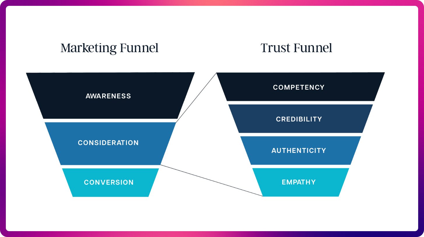
营销漏斗?不,现在是信任漏斗
做营销这么多年,我发现很多所谓的“规则”和“玩法”其实都搞错了重点。我们总是在解释我们做什么,为什么重要。
但在大多数情况下,你的潜在客户早就知道他们需要你卖的东西。
他们根本不需要再看一份PPT,来了解AI编码助手如何提升开发效率,也不需要你告诉他们AI销售代表为什么可以帮他们发更多邮件。
过去一个月,他们可能已经听了40次这样的东西(天啊,现在到底有多少AI销售代表啊?)。
他们真正想知道的是:“凭什么我要跟你买,而不是另外100家发同样邮件来骚扰我的公司?”
而现在,铺天盖地的AI内容,让客户更难回答这个问题了。
图1 是我从PHOS Creative那里借用的:
(图片描述:
营销漏斗(Marketing Funnel)
- 品牌认知 / 触达(Awareness)
- 评估 / 意向(Consideration)
- 转化 / 下单(Conversion)
信任漏斗(Trust Funnel)
- 能力 / 胜任度(Competency)
- 可信度 / 公信力(Credibility)
- 真实感 / 真实性(Authenticity)
- 共情 / 同理心(Empathy)
)
维度
- 核心关注
* 营销漏斗:获客和转化
* 信任漏斗:建立关系和客户忠诚
- 最终目标
* 营销漏斗:完成交易
* 信任漏斗:长期客户支持与复购
- 内容策略
* 营销漏斗:推广为主,销售导向
* 信任漏斗:帮助客户,创造价值
- 衡量成功
* 营销漏斗:转化率、销量
* 信任漏斗:满意度、重复购买、口碑传播
-时间跨度
* 营销漏斗:短期到中期
* 信任漏斗:长期、持续积累信任
很明显,你应该站到信任那一边!
传统的获客方式现在变得很烂
现在这种获客方式实在是太无聊了。
当Claude的AI授权只需每月10美元时,内容创作成本基本为零。于是所有人都可以装得很专业,邮件里每个字语法正确,还能勉强引用你的领英发帖(虽然引用得很僵硬)。
这些东西几分钟就能生成,不用任何人工参与。
这就意味着:现在所有内容都值得怀疑。
现在,我直接把邮件和领英消息一律扔进垃圾桶。
为什么?因为我一眼就能看出,那背后并不是一个真正关心我和我的问题的人。
这些邮件全都是模糊的“个性化”,总是自称“对你如何做某件事感到好奇”,因为这种“好奇”的句式来自某个声称效果很好的推广指南。
对我来说,这就是信任崩塌的关键:
我并不是怀疑你的产品能不能用,我是怀疑你到底是不是个真人,签完合同后还会不会关心我。
响应率低了,我多发点邮件就好了?
天啊,别这样!
问题根本不在这里。
旧世界 (…-2024年)
* 创造可信、个性化内容的成本:50美元/小时(人工)
* 用户每周收到的个性化推广邮件:约10封
* 用户识别真实性的成功率:约80%
新世界 (2025年-…)
* 创造可信、个性化内容的成本:几乎为0
* 用户每周收到的个性化推广邮件:约200封
* 用户识别真实性的成功率:约20%
信噪比已经崩溃,识别这些邮件真实性的精力成本远超过可能获得的收益。
结果,客户不再费力去判断真假,而直接默认这些全是垃圾邮件。这也是为什么我和我朋友干脆无视所有推广邮件的原因——很多人也一样。
因为要辨别“这些邮件里有没有价值”,所耗费的精力早就远远超过了可能获得的好处。
回到信任本身…
你必须明白,你的潜在客户问的不是:
* 你的AI工具好不好用?(他们默认你的工具好用)
* 真的能提升效果吗?(他们默认有效果)
* 价格合适吗?(他们自己能对比)
他们真正关心的是:
* 一年后你公司还在吗?还是集成到一半你就跑路了?
* 你到底比另外5家公司好在哪里?
* 你是不是靠烧VC的钱活着?
* 等到风口过去,我的系统是不是会烂尾?
* 你们公司到底赚不赚钱?还是只是凭感觉(vibe-coded,凭感觉编程,意为没有实际盈利模型、靠炒作存活的公司)想赶紧卖掉?
而最糟糕的是:如果你不明确告诉客户,他们根本没法自己判断这些问题。
不是想泼冷水,但…
我写这篇文章不是为了打击你,而是为了让你知道现在的营销要怎么玩。
是的,你依然要回答“客户为什么需要你的产品”,但你更要回答“客户为什么必须跟你买”,并确保你的营销内容体现这一点。
机遇仍然很大。我们所有人都必须做到:
* 信任的建立,仍然是人类的工作。至少现在还是。AI能帮忙,但2025年建立真正的情感联结和信任,仍然只能靠人类。
* 个性化和精准营销依旧重要。AI应该帮你精细分类客户,但重点仍是识别什么时候该由人类出面,强化信任。
* 别把所有事情都自动化。尤其是复杂或高价值的销售场景,保持一定的人类参与至关重要。
AI时代真的不同了吗?
当然。
你代表一个品牌。品牌要持续赢得客户的信任——即使你使用了AI,也必须清晰体现出人类的领导力与温度。
来源:arnon.dk/the-trust-collapse-…

scott retweeted

🦔DoubleLine Capital warns fixed-income investors to be cautious about AI debt as Alphabet sold $17.5 billion in US bonds, Meta raised $30 billion after a $27 billion private sale, and Oracle tapped $18 billion in September. Director Robert Cohen asks: "Who knows what the spillover will be if the music stops?"
The $3 Trillion Problem
Morgan Stanley forecasts hyperscalers will spend $3 trillion on infrastructure through 2028. Cash flow can fund about half, requiring significant debt issuance. Cohen warned about novel off-balance sheet structures and noted no one knows if these projects will be profitable. DoubleLine clients that committed capital to private credit have been disappointed and are seeking to diversify away from it.
My Take
DoubleLine's credit director is flagging exactly what I've been discussing about spillover risks. Cohen's warning that if most projects aren't profitable there will be a severe reaction matters because major credit investors are positioning defensively. His clients being disappointed with private credit adds to TCW being 15% underweight and Deutsche Bank hedging AI exposure. Morgan Stanley forecasting $3 trillion in spending with half requiring debt while no one knows if projects will be profitable creates the leverage problem. Off-balance sheet structures mean losses materialize before they're visible.
Hedgie🤗

scott retweeted
Elemental Abundance of Earth
This is quite an important chart to understand the progress of humanity and maybe identify some things that we might have skipped over in our tech tree progress as a civilisation.
Here’s how to read it.
The X axis is all the naturally occurring elements ranked by their atom number (size of their nucleus). Small atoms on left, big atoms on right.
The Y axis is logarithmic and tells you the abundance of each element in the Earth’s crust.
Side note: All of these elements (other than hydrogen) were made inside an old star that existed before our sun and exploded in a supernova. Our planet is made from the ashes of a dead star.
Now different planets that orbit our sun have different orbit distances and at diff distances there are different combinations of all these elements to form each planet.
The chart below is what we rolled for Earth. Some stuff is very abundant, some stuff is rare.
Now, if you think about this from a high level, the stuff that is very common, should be easily come by, it should be readily available to Earthlings, it should be relatively cheap.
Stuff that is rarer should be harder to find, should be less available should naturally be more expensive.
Stuff that is cheap should be very economic for us to use, we should therefore use more of that stuff and we should therefore get really good at working with that stuff.
Stuff that is harder to find, stuff that is therefore relatively expensive would also be stuff that we use less (economic reasons), and therefore we get less good at using that stuff.
This are very general rules that should apply to any civilisation on any planet at any stage of development. You might be able to estimate what sort of materials and technologies a civilisation on a far away planet would be more likely to develop based purely on the abundance profile of their home world.
You can also look introspectively and check are the elements that are most abundant on Earth also the ones that form the cheapest materials in our economy? Did we get good with the thing easier to get good at on Earth? If not why not? Because maybe there’s a huge opportunity there.
This suggests we are underachieving with our use of magnesium, titanium, calcium, sodium, sulphur.
We are overachieving with our use of copper, lithium, silver, nitrogen, carbon, nickel, cobalt.
Human civilisation is currently over optimised for extraction and use of rare conductive and catalytic elements, and we are under optimised for use of our abundant lightweight reactive elements.
Why has this happened?
1. Economic inertia, iron and copper matured before titanium and magnesium.
2. Chemical accessibility, oxides and silicates demand high energy reduction.
3. Utility density, because of transport costs we value compact specific systems rather than bulk designs.
4. Historic lock in, infrastructure path dependence (steel - cu - al).
If we were more rationally utilised…
Structural alloys, we still use Fe and Al when Ti and Mg are superior and more abundant.
Batteries, we use Li and Co when Na, Mg, Al should be more economic.
Catalysis, we use Pt, Rd, Rh when we should be using Ti, Fe, Mo, W, nitrides.
Electronics, we use Cu when Al and graphene should be more economical.
There are myriad reasons for all these but it’s down to economic drivers and usually because we lack some technological step to bring the more abundant material to our economy more efficiently.
Overall this suggests our entire process chemistry industry is not performing for humanity as well as it could. Although we have no alien civilisation for any frame of reference, so maybe we are doing well?
But this exercise shows our economy and material use has massive economic opportunities to rebalance our economy’s material demands to reflect the resource wealth of Earth.
We should think about this much more deeply as we look to develop other worlds and moons.

scott retweeted

Nugget from a survey of 149 senior data-center/energy professionals.
"44% indicate average quoted utility wait times of 4 years"

scott retweeted

🏗️ A Goldman Sachs research estimates that AI could automate work equal to 300 million full time jobs, with the biggest hit on desk jobs and far less on hands on trades.
46% exposure for office and administrative support, 44% for legal, 37% for architecture and engineering, while construction and maintenance sit near 6% or lower.
“Exposure” here means a large chunk of day to day tasks can be done by software, not that all those jobs go away at once.
Knowledge jobs rank high because their core tasks live in text, code, documents, meetings, and rules, which are exactly what large language models and related tools can read, write, summarize, and reason over.
Physical jobs rank low because they require movement in messy real spaces, use of tools, safety judgment, and customer interaction that current robots and perception systems still struggle to do reliably and cheaply.
Think of AI first eating routine cognitive tasks like drafting emails, writing first pass contracts, summarizing cases, creating specs, extracting data from forms, and checking compliance, which compresses time and headcount needs inside those functions.

scott retweeted

China is a manufacturing powerhouse, yet it has low productivity per traditional analysis.
But when you look at actual physical output per worker, China’s labor productivity is far higher than traditional estimates.
Outstanding piece by Weijian Shan: research.gavekal.com/article…


We just published a terrific guest piece from my friend Weijian Shan. I think it is a must read for anyone looking to understand China’s advances in manufacturing.
research.gavekal.com/article…
The piece has no firewall and is open to everyone.
Incidentally, Weijian Shan wrote one of my favourite books; a book I had all four of my kids read. The book, OUT OF THE GOBI, details his growing up at the time of the cultural revolution. Hard to understand China today without understanding what the current generation of leaders went through in the late 1960s/early 1970s…
Please forward widely!
scott retweeted

Just how much are we spending on AI?
Compared to other massive infrastructure projects, AI is the sixth largest in US history, so far.
World War II dwarfs everything else at 37.8% of GDP. World War I consumed 12.3%. The New Deal peaked at 7.7%. Railroads during the Gilded Age reached 6.0%.
AI infrastructure today sits at 1.6%, just above the telecom bubble’s 1.2% & well below the major historical mobilizations.
Companies like Microsoft, Google, & Meta are investing $140B, $92B, & $71B respectivelyin data centers & GPUs. OpenAI plans to spend $295B in 2030 alone.
If we assume OpenAI represents 30% of the market, total AI infrastructure spending would reach $983B annually by 2030, or 2.8% of GDP.
To match the railroad era’s 6% of GDP, AI spending would need to reach $2.1T per year by 2030 (6% of projected $35.4T GDP), a 320% increase from today’s $500B. That would require Google, Meta, OpenAI, & Microsoft each investing $500-700B per year, a 5-7x increase from today’s levels.
And that should give you a sense of how much we were spending on railroads 150 years ago!
tomtunguz.com/llm-impact-gdp…


scott retweeted

With the growth of AI data centers, there's been a lot of talk about America's pivot to natural gas power.
But renewables continue to dominate the US power sector. 93% of capacity built in the last 12 months came from solar, wind and batteries.
🧵

scott retweeted
📈 WOW. Google is finally rolling out its most powerful Ironwood AI chip, first introduced in April, taking aim at Nvidia in the coming weeks.
Its 4x faster than its predecessor, allowing more than 9K TPUs connected in a single pod.
The big deal is that many are not realizing, if it can do an all-reduce across 9k TPUs, it can run MUCH larger models than the Nvidia NVL72.
It would make really big 10T param size models like GPT-4.5 feasible to run. It’d make 100T param size models possible.
This is the last big push to prove that scaling works. If Google trains a 100T size model and demonstrates more intelligence and more emergent behavior, the AGI race kicks into another gear. If 100T scale models just plateau, then the AI bubble pops.
---
Ironwood TPUs go GA and Axion Arm VMs expand, promising upto 10X gains and cheaper inference while adding flexible CPU options for the boring but vital parts of AI apps.
Ironwood targets both training and serving with 10X peak over v5p and 4X better per chip than v6e for training and inference, so the same hardware can train a frontier model and then serve it at scale.
A single superpod stitches 9,216 chips with 9.6 Tb/s Inter-Chip Interconnect and exposes 1.77PB of shared HBM, which cuts cross device data stalls that usually throttle large models.
Optical Circuit Switching reroutes around failures in real time and the Jupiter fabric links pods into clusters with hundreds of thousands of TPUs, so uptime and scale do not fight each other.
On software, Cluster Director in GKE improves topology aware scheduling, MaxText adds straightforward paths for SFT and GRPO, vLLM runs on TPUs with small config tweaks, and GKE Inference Gateway cuts TTFT by up to 96% and serving cost by up to 30%.
Axion fills the general compute side of the house so data prep, ingestion, microservices, and databases stay fast and cheap while accelerators focus on model math.
N4A, now in preview, offers up to 64 vCPUs, 512GB memory, 50Gbps networking, custom machine types, and Hyperdisk Balanced and Throughput, aiming for about 2x better price performance than similar x86 VMs.
C4A Metal, in preview soon, gives dedicated Arm bare metal with up to 96 vCPUs, 768GB memory, Hyperdisk, and up to 100Gbps networking for hypervisors and native Arm development.
C4A provides steady high performance with up to 72 vCPUs, 576GB memory, 100Gbps Tier 1 networking, Titanium SSD up to 6TB local capacity, advanced maintenance controls, and support for Hyperdisk Balanced, Throughput, and Extreme.


Our 7th gen TPU Ironwood is coming to GA!
It’s our most powerful TPU yet: 10X peak performance improvement vs. TPU v5p, and more than 4X better performance per chip for both training + inference workloads vs. TPU v6e (Trillium). We use TPUs to train + serve our own frontier models, including Gemini, and we’re excited to make the latest generation available to @googlecloud customers.